

pcb and pcba components identified on the silkscreen layer
In the intricate world of printed circuit boards (PCBs) and printed circuit board assemblies (PCBAs), where every component plays a crucial role in shaping functionality and performance, accurate identification of components is paramount. Among the various layers that comprise a PCB or PCBA, the silkscreen layer stands out as a vital tool for conveying essential information about the components populating the board. Let’s delve into the mechanisms by which PCB and PCBA components are identified and delineated on the silkscreen layer.
The silkscreen layer serves as a visual guide, offering a roadmap for assembly technicians and engineers to navigate the labyrinth of components adorning the pcb and pcba. Through a combination of symbols, text, and graphical elements, the silkscreen provides critical information such as component outlines, reference designators, polarity indicators, and pinout diagrams. These markings are strategically placed alongside each component, ensuring clear and concise identification even amidst a sea of intricate circuitry.
One of the primary methods used to identify components on the silkscreen layer is through reference designators. Reference designators are alphanumeric labels assigned to each component on the PCB or PCBA, enabling easy identification and cross-referencing with schematic diagrams and bill of materials (BOM). These labels typically consist of a prefix indicating the component type (e.g., R for resistors, C for capacitors, U for integrated circuits) followed by a unique numerical identifier. By correlating reference designators with component values and locations, assembly technicians can quickly locate and populate the board with the requisite components.
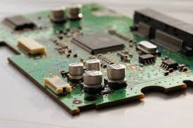
How are pcb and pcba components identified on the silkscreen layer?
In addition to reference designators, the silkscreen layer often incorporates component outlines to visually depict the footprint and orientation of each component. These outlines serve as a visual aid, guiding assembly technicians in accurately placing components on the board and ensuring proper alignment with solder pads and mounting holes. By providing a clear delineation of component boundaries, the silkscreen minimizes the risk of assembly errors and ensures optimal component placement, thereby enhancing the functionality and reliability of the final product.
Furthermore, polarity indicators are commonly used on the silkscreen layer to denote the orientation of polarized components such as diodes, electrolytic capacitors, and LEDs. These indicators, often depicted as arrows, dots, or other graphical symbols, help assembly technicians align components correctly with respect to their polarity markings, thereby preventing polarity reversal and ensuring proper functionality of the circuit. This simple yet effective visual cue mitigates the risk of installation errors and minimizes the likelihood of premature component failure due to incorrect polarity.
Pinout diagrams are another valuable feature found on the silkscreen layer, particularly for complex components such as integrated circuits (ICs) and connectors. These diagrams provide a graphical representation of the pin assignments and functions of each component, aiding assembly technicians in correctly soldering and interconnecting the pins with other components or external devices. By offering a visual roadmap of the component’s electrical connectivity, pinout diagrams streamline the assembly process and minimize the risk of wiring errors or signal misrouting.
In conclusion, the silkscreen layer of a PCB or PCBA serves as a critical tool for identifying and delineating components, facilitating efficient assembly and ensuring the integrity and functionality of the circuitry. Through a combination of reference designators, component outlines, polarity indicators, and pinout diagrams, the silkscreen layer provides assembly technicians with essential information to navigate the complexities of electronic assembly with precision and confidence. As technology continues to advance, the importance of clear and accurate component identification on the silkscreen layer will remain indispensable in the realm of electronic design and manufacturing.