

EMI/RFI Shielding in PCB Board Manufacturers
If you’re a pcb board manufacturer, chances are that you must be aware of the impact of electromagnetic interference (EMI). In fact, EMI is a critical aspect of PCB design. It prevents signals from interfering with each other and also prevents stronger signals from overpowering smaller ones. To minimize EMI, a number of different strategies must be applied. This includes using shields to keep the components of a circuit board apart, minimizing traces’ lengths to reduce their inherent capacitance, ensuring the proper grounding of all signals, and keeping high-speed traces adjacent to the ground plane in order to minimize cross-talk.
Another key to ensuring that a pcb board manufacturer will be free from EMI is incorporating filtering components, like ferrite beads and EMI filters, into the design. These devices will eliminate the noise from the higher-speed signals and prevent them from causing conducted EMI. The use of these components is especially important in industrial PCBs, where the data generated by the system must be accurate and clear in order to make decisions and take action that will affect the safety of people, property and equipment.
In addition to these filtering components, a good PCB design will have adequate metal shielding to minimize conducted and radiated EMI. Shielding can be made of either solid copper or a combination of solid and cross-hatched copper layers. The solid copper layer provides a higher level of shielding, while the cross-hatched layers allow flexibility in the board.
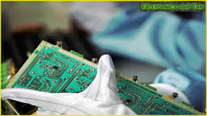
How to Ensure EMI/RFI Shielding in PCB Board Manufacturers
EMI shielding is an essential part of any electronic design, and can be used to protect the sensitive electronics in a wide range of applications. From personal electronics to power supplies and telecommunications systems, it’s important to have shielding in place to prevent interference from outside sources. It’s important to note that EMI can also be produced internally by the electronics in a circuit board, so ensuring the proper layout and component placement is crucial to prevent EMI production.
Grounding: Almost all EMI problems can be traced back to poor grounding, so the first step to eliminating EMI is to create a solid and consistent ground potential throughout the PCB stackup. This will prevent common-mode noise circulation, signal reflection and RF interference.
Trace length: A PCB’s conductive paths, known as traces, are one mistake away from being radiating antennas. To avoid this, it’s important to keep traces as short and as parallel as possible. Also, if the traces must intersect, make sure to round out any corners to minimize the effect on characteristic impedance.
Incorporate these tips into your next PCB layout to ensure that your products will be free from EMI and RFI interference. If you’re interested in learning more about how to implement these PCB design tips and other EMC design considerations, check out Altium Designer. This PCB software offers the advanced features needed to create a top-notch design and analyze it for performance. If you have any questions, reach out to our team of experts. We’re always happy to help!